News
Application of High Voltage Power Supply in Semiconductor Processing
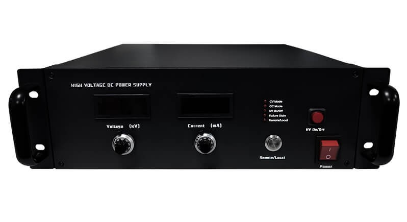
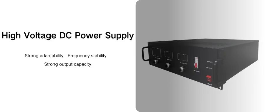
In the processing of semiconductor chips, high-voltage power supplies play an important role and are widely used in various precision machining and testing equipment.
1. Ion implantation
Ion implantation is a process of altering the electrical properties of semiconductor materials through bombardment techniques. In this process, the high-voltage power supply provides an acceleration voltage of 20-200 kV to the ion implantation equipment, allowing the injected ions to obtain sufficient kinetic energy to be injected into the interior of the target material. By accelerating and injecting the ions into the semiconductor chip, their electrical properties can be changed.
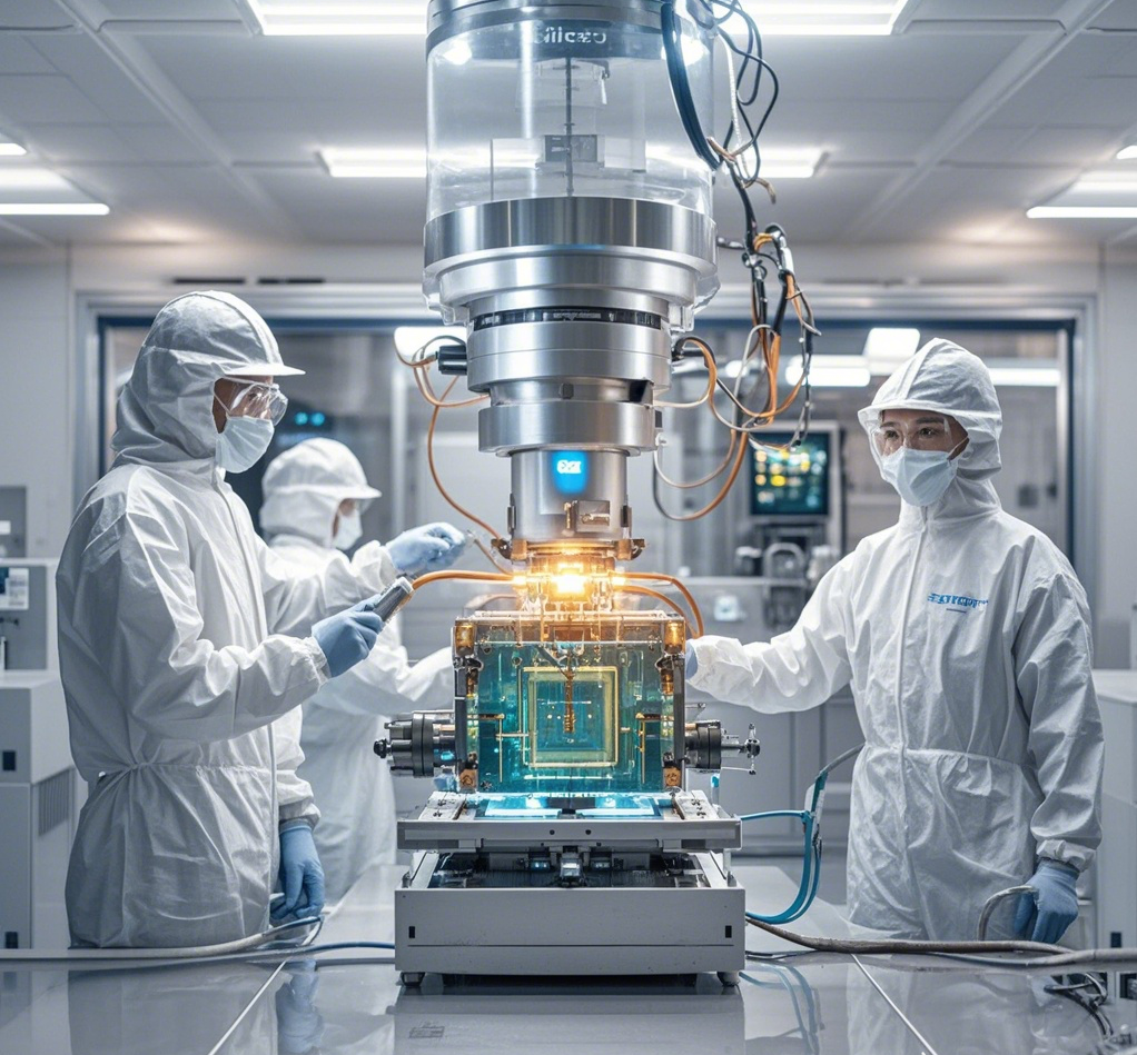
The output voltage of a high-voltage power supply is directly related to the energy of the injected ions, thereby determining the depth and dose distribution of the injection. It controls the acceleration and orientation of ions by generating a strong electric field, ensuring accurate ion injection into the target area. The stability of the high-voltage power supply directly affects the injection uniformity. Therefore, the voltage accuracy and stability of high-voltage power supply are crucial to ensuring the quality of ion implantation.
2. Ionic film formation
Ionic film formation is a crucial process in semiconductor technology, used to deposit thin films on the surface of semiconductor chips, which can be insulating layers, conductive layers, or semiconductor layers. This process requires the use of high-voltage direct current discharge to generate plasma, which is then deposited on the wafer surface through plasma collision reactions to form various thin films.
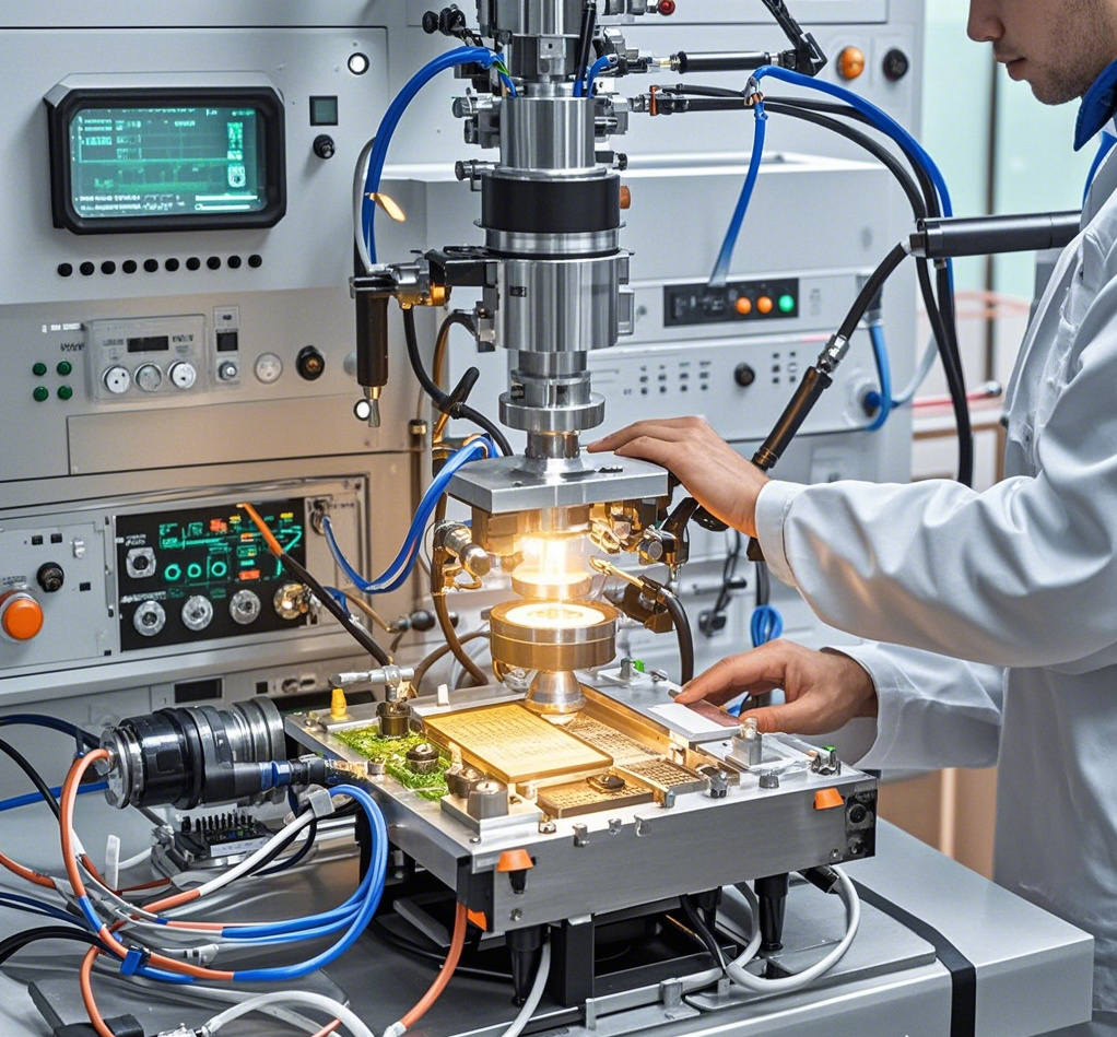
In ion deposition equipment, the high-voltage power supply generates a direct current high voltage of 1-5 kV, which is used to ignite the discharge electrode and generate plasma. The high-voltage power supply adjusts the electric field strength by precisely controlling the output voltage, helping to control the deposition rate and uniformity of the thin film, accurately controlling the composition of the plasma, thereby ensuring that the thin film is uniformly deposited on the surface of the chip and reaches the required thickness, ensuring the quality of film formation.
3. Electron beam lithography
Electron beam lithography is an important photolithography technique that uses focused electron beams to accurately remove semiconductor materials and directly depict semiconductor chip patterns. It utilizes the bombardment effect of high-energy electron beams to directly depict fine patterns and structures on electron sensitive resists.

In this technology, the high-voltage power supply generates a DC high voltage of 5-50 kV as the acceleration voltage for the electron gun. The generated plasma will react with the surface of semiconductor materials to remove unwanted materials. The stability of voltage directly affects the stability of electron beam parameters, which in turn affects the accuracy of depiction. At the same time, the high-voltage power supply also needs to provide various bias and focusing voltages.
In summary, high-voltage power supply is an essential energy source and control platform for various precision equipment in the semiconductor manufacturing process. Semiconductor manufacturers need to select high-voltage power supplies with parameter matching, stable and reliable performance to meet the precise control requirements of processing equipment and ensure the quality of semiconductor processes and products.
RELATED NEWS
- IDEALPLUSING | Electrospinning 2024-10-29
- Application of High Voltage Power Supply in Wind Farm 2024-09-20
- Application of non-destructive testing for high-voltage power supply 2024-09-19
- Application of High Voltage Power Supply in Electron Beam Welding 2024-09-18
- Detailed description of ripple in high-voltage power supply 2024-09-14
CATEGORIES
LATEST NEWS
CONTACT US
Contact:
Phone: +86-158-7657-0341
E-mail: market@jmhvpower.com
Whatsapp:+86-158-7657-0341
Add: Guangdong Province, China TianHe District, GuangZhou Num 899
