Industry news
Calculation of PCB parasitic capacitance and parasitic inductance
In high-speed or high-frequency circuit boards, the parasitic effects in the PCB are very obvious. These parasitic capacitance and parasitic inductance can cause crosstalk, EMI, signal integrity and other problems. When dealing with high-frequency, high-speed and mixed-signal PCBs, some special treatments are needed to reduce the impact of parasitic effects on the signals.
In order to reduce the impact of parasitic capacitance and inductance, we need to know how they are generated so that we can prescribe the right medicine. In this section, we first learn how to calculate the parasitic capacitance and parasitic inductance of PCBs, and then discuss how to reduce their impact.
Conductors on PCBs generally have traces and vias (pads, copper cladding, etc. can be equivalent to traces). The structures of the two are completely different, so when we discuss parasitic effects, we need to analyze these two structures separately.
1) Parasitic capacitance
Parasitic capacitance of signal lines/pads:
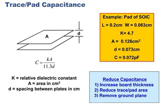
We know that the capacitance calculation formula of a flat plate capacitor is: C=ε0*S/d; where ε0 is the dielectric constant, S is the area of the two opposite plates, and d is the distance between the two plates. It can be seen that, under the condition of a constant dielectric constant, the larger the area S facing each other and the smaller the distance d, the greater the capacitance.
Since the equivalent facing area between signal lines on the same layer of the PCB is very small, and the distance is also large relative to the spacing between adjacent layers, the parasitic capacitance between the traces in the same layer is considered to be very small and can be ignored; the area covered by the trace is regarded as the area of the flat plate capacitor, the spacing between adjacent layers is regarded as the spacing of the flat plate capacitor, and the small capacitance caused by other factors is ignored, and the generation of parasitic capacitance can be simplified to the capacitance of the flat plate capacitor.
It can be calculated as shown below: (A is the area, d is the distance from the adjacent reference layer, and K=4.7 in the example takes the dielectric constant of the PCB board into account)

From this calculation formula, it can be seen that if you want to reduce the parasitic capacitance of signal lines and pads, when designing PCB, one is to reduce the total area covered by the copper foil; the other is to increase the layer spacing (in actual operation, you can choose a PCB stacking structure with a large layer spacing, or hollow out the reference surface of the adjacent layer)
Parasitic capacitance of vias:
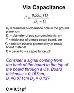
The parasitic capacitance of vias cannot be equivalent to a flat capacitor, and is generally calculated using the following formula:
(Where D1 is the outer diameter of the via, D2 is the circular diameter of the hollowed-out copper foil around the via, T is the PCB thickness, and εr is the relative magnetic permeability of the board)
From the above calculation formula, it can be seen that in order to reduce the parasitic capacitance of vias, it is necessary to use vias with small apertures, increase the spacing between vias and copper foil, and choose thinner PCB boards.

2) Parasitic inductance
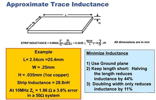
The calculation method of the parasitic inductance of the signal line/pad is as follows: (W is the line width, L is the line length, and H is the copper thickness)

This formula looks complicated. In fact, the line length L has the greatest impact on the parasitic inductance. Shortening the length of L is the most effective way to reduce the parasitic inductance of the signal line.
Parasitic inductance of vias:
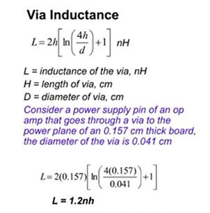
The calculation method is as follows: (h is the board thickness, D is the via diameter)

From the formula, it can be seen that to reduce the parasitic inductance of the via, it is necessary to reduce the board thickness and increase the via diameter.
RELATED NEWS
- IDEALPLUSING Working principle of inductor 2024-08-15
- What is the difference between meltblown cloth and non-woven fabric? 2024-08-14
- High-frequency multiple high-voltage pulse power supply for dust collector 2024-07-17
- What is a high-voltage pulse power grid? Working principle of high-voltage pulse 2024-07-12
- Application of high voltage power supply in the field of X-ray instrument 2024-07-11
CATEGORIES
LATEST NEWS
CONTACT US
Contact:
Phone: +86-158-7657-0341
E-mail: market@jmhvpower.com
Whatsapp:+86-158-7657-0341
Add: Guangdong Province, China TianHe District, GuangZhou Num 899
