Industry news
Uncover the mystery of mos tube damage
The first: avalanche damage
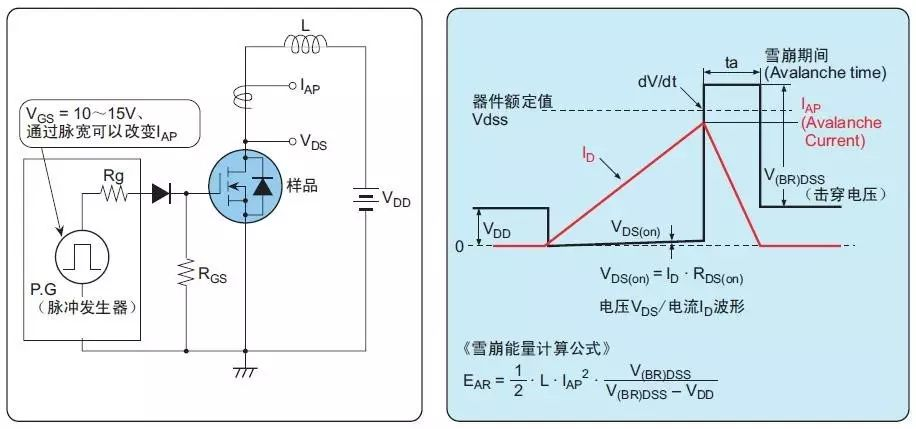
If the drain-source surge voltage exceeds the rated VDSS of the device, and reaches the breakdown voltage V(BR)DSS (according to the breakdown current, the value is different), and exceeds a certain amount of energy after the destruction of the phenomenon.
Avalanche damage occurs when the switching operation of the dielectric load is switched off, or when the spike voltage generated by the magnetic leakage inductance exceeds the rated drain withstand voltage of the power MOSFET and enters the breakdown region, resulting in a damage mode.
Typical circuit:
The second type: device heat damage
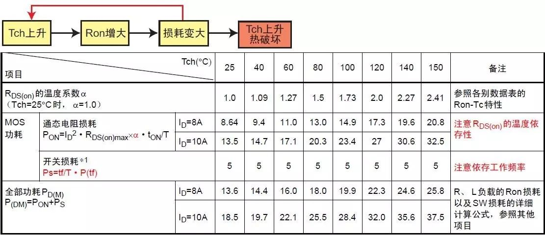
Caused by exceeding the safety zone caused by heat generation. The cause of heat generation is categorized into DC power and transient power.
DC power causes: the loss caused by the external DC power caused by heat generation
On-resistance RDS(on) loss (RDS(on) increases at high temperatures, resulting in an increase in power consumption at a certain current)
Losses caused by leakage current IDSS (very small compared to other losses)
Transient power cause: external single trigger pulse
Load short circuit
Switching losses (on, off) * (temperature and operating frequency dependent)
trr losses of built-in diodes (short-circuit losses of upper and lower bridge arms) (temperature and operating frequency dependent)
Overcurrents caused by load short circuits, etc. that do not occur during normal operation of the device cause transient localized heating that leads to damage. In addition, due to heat mismatch or switching frequency is too high so that the chip can not be normal heat dissipation, the continuous heat so that the temperature exceeds the channel temperature leading to destruction of thermal breakdown.
The third type: built-in diode damage
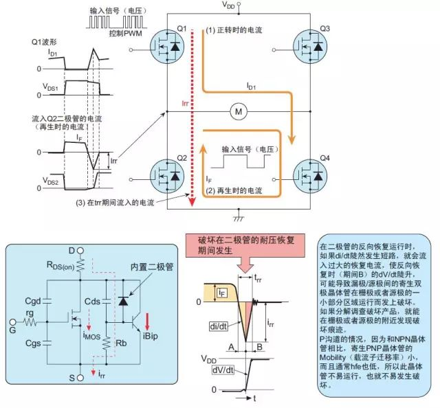
When the parasitic diode constituted between the DS terminals is operated, due to the operation of the parasitic bipolar transistor of the power MOSFET at the Flyback
This diode destruction mode is caused.
Fourth type: Destruction caused by parasitic oscillation
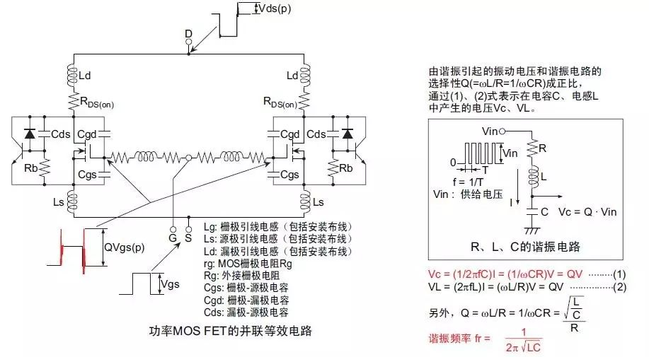
This mode of destruction is especially likely to occur when connected in parallel.
Gate parasitic oscillation occurs when a power MOS FET is connected directly in parallel without inserting a gate resistor. This parasitic oscillation occurs on the resonant circuit formed by the gate-drain capacitance Cgd(Crss) and the gate pin inductance Lg when the drain-source voltage is repeatedly turned on and off at high speed. When the resonance condition (ωL=1/ωC) is established, a vibration voltage much larger than the driving voltage Vgs(in) is applied externally across the gate-source, and the gate may be damaged due to exceeding the rated voltage across the gate-source, or the vibration voltage at the time of switching on and switching off the voltage across the drain-source may cause a positive feedback through the overlap of the waveforms of the gate-drain capacitance Cgd and Vgs, and may thus cause due to malfunctioning of the Oscillation damage.
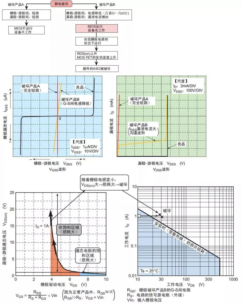
Fifth: gate surge, electrostatic damage
To have due to the gate and the source if there is a voltage surge between the gate and the source and the damage caused by static electricity, that is, gate over-voltage damage and by the power-up state in the electrostatic charge at both ends of the GS (including the installation and and the measurement of the equipment charged) and lead to the gate damage.
RELATED NEWS
- IDEALPLUSING Working principle of inductor 2024-08-15
- What is the difference between meltblown cloth and non-woven fabric? 2024-08-14
- Calculation of PCB parasitic capacitance and parasitic inductance 2024-07-19
- High-frequency multiple high-voltage pulse power supply for dust collector 2024-07-17
- What is a high-voltage pulse power grid? Working principle of high-voltage pulse 2024-07-12
CATEGORIES
LATEST NEWS
CONTACT US
Contact:
Phone: +86-158-7657-0341
E-mail: market@jmhvpower.com
Whatsapp:+86-158-7657-0341
Add: Guangdong Province, China TianHe District, GuangZhou Num 899
